

How an IGBT works: Structure, Construction, Advantages & Application

How an IGBT works – Introduction:
IGBT is a three-terminal power semiconductor device primarily used as an electronic switch. In this article let’s see How an IGBT works, Its Construction, Advantages and also its Application
Full form of IGBT
Full form of IGBT is Insulated Gate Bipolar Transistor (IGBT)
What is an IGBT?
- IGBT is a minority-carrier device with high input impedance and large bipolar current-carry.
- Many designers view IGBT as a device with MOS input characteristics and bipolar output characteristic that is a voltage-controlled bipolar device.
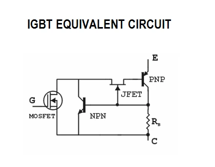
- To make use of the advantages of both Power MOSFET and BJT, the IGBT has been introduced. It’s a functional integration of Power MOSFET and BJT devices in monolithic form. It combines the best attributes of both to achieve optimal device characteristics.
IGBT usage
- The IGBT is suitable for many applications in power electronics, especially in Pulse Width Modulated (PWM) servo and three-phase drives requiring high dynamic range control and low noise.
- It also can be used in Uninterruptible Power Supplies (UPS), Switched-Mode Power Supplies (SMPS), and other power circuits requiring high switch repetition rates.
- IGBT improves dynamic performance and efficiency and reduced the level of audible noise. It is equally suitable in resonant-mode converter circuits. Optimized IGBT is available for both low conduction loss and low switching loss.
What is the advantage of IGST
Advantages of IGBT
- It has a very low on-state voltage drop due to conductivity modulation and has superior on-state current density. So smaller chip size is possible and the cost can be reduced.
- Low driving power and a simple drive circuit due to the input MOS gate structure. It canbe easily controlled as compared to current controlled devices (thyristor, BJT) in high voltage and high current applications.
- Wide SOA. It has superior current conduction capability compared with the bipolar transistor. It also has excellent forward and reverse blocking capabilities.
Drawbacks of IGBT
- Switching speed is inferior to that of a Power MOSFET and superior to that of a BJT. The collector current tailing due to the minority carrier causes the turnoff speed to be slow.
- There is a possibility of latchup due to the internal PNPN thyristor structure
Construction and Working of IGBT
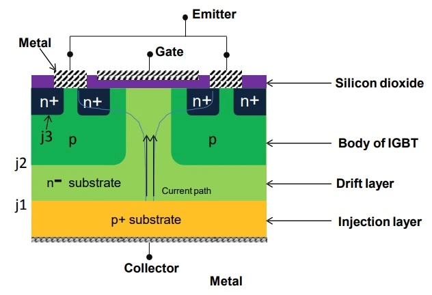
The structure of IGBT is very much similar to that of Power MOSFET, except one layer known as injection layer which is p+ unlike n+ substrate in PMOSFET. This p+ injection layer is the key to the superior characteristics of IGBT. It injects holes into n- layer. Thickness of n- layer decides the voltage blocking capability. Other layers are called the drift and the body region. The two junctions are labelled J1 and J2
How an IGBT works?
IGBT Working
- N-channel IGBT turns ON when the collector is at a positive potential with respect to emitter and gate also at sufficient positive potential (>VGET) with respect to emitter. This condition leads to the formation of an inversion layer just below the gate, leading to a channel formation and also a current begins to flow from collector to emitter. This n- channel short circuits the n+ with n- emitter regions.
- Electrons from emitter n+ region flows to n drift region through n-channel. The collector current Ic in IGBT constitutes of two components- Ie and Ih. Ie is the current due to injected electrons flowing from collector to emitter through injection layer, drift layer and also finally the channel formed. Ih is the hole current flowing from collector to emitter through Q1 and body resistance Rb.
IGBT characteristics:
Let’s see the IGBT characteristics
Output Characteristics:
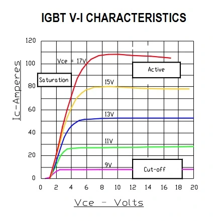
The plot for forward output characteristics of an NPT-IGBT is shown in Figure. It has a family of curves, each of which corresponds to a different gate-to-emitter voltage (VGE). The collector current (IC) is measured as a function of collector-emitter voltage (VCE) with the gate-emitter voltage (VGE) constant.
Transfer Characteristics:
The transfer characteristic is defined as the variation of ICE with VGE values at different temperatures. A typical transfer characteristic is shown in Figure. The gradient of transfer characteristic at a given temperature is a measure of the transconductance (gfs) of the device at that temperature.
Switching Characteristics:

The switching characteristics of an IGBT are very much similar to that of a Power MOSFET. The major difference from Power MOSFET is that it has a tailing collector current due to the stored charge in the N- -drift region. The tail current increases the turnoff loss and requires an increase in the dead time between the conduction of two devices in a half-bridge circuit. The Figure shows a test circuit for switching characteristics and also the corresponding current and voltage turn-on and turn-off waveforms. IXYS IGBTs are tested with a gate voltage switched from +15V to 0V. To reduce switching losses, it is recommended to switch off the gate with a negative voltage (-15V).
Applications of IGBT
IGBT finds its use in medium power applications like
- DC and AC motor drives
- Medium power supplies
- Solid state relays
- General purpose inverters
- UPS
- Welder equipment
- Servo controls
- Robotics
- Cutting tools
IGBT FAQ
What is an IGBT used for?
Insulated Gate Bipolar Transistor is a three-terminal power semiconductor device primarily used as an electronic switch. The IGBT is suitable for many applications in power electronics, especially in Pulse Width Modulated (PWM) servo and three-phase drives requiring high dynamic range control and low noise
What is the advantage of IGBT?
- It has a very low on-state voltage drop due to conductivity modulation and has superior on-state current density. So smaller chip size is possible and the cost can be reduced.
- Low driving power and a simple drive circuit due to the input MOS gate structure. It canbe easily controlled as compared to current controlled devices (thyristor, BJT) in high voltage and high current applications.
- Wide SOA. It has superior current conduction capability compared with the bipolar transistor. It also has excellent forward and reverse blocking capabilities.
Why IGBT is used instead of MOSFET?
To make use of the advantages of both Power MOSFET and BJT, the IGBT has been introduced. It’s a functional integration of Power MOSFET and BJT devices in monolithic form. It combines the best attributes of both to achieve optimal device characteristics.
How IGBT turn on and off?
The Insulated Gate Bipolar Transistor (IGBT) can be switched ‘ON’ and ‘OFF’ by activating the gate.
What is the working principle of IGBT?
IGBT working principle is based on the biasing between Gate-Emitter terminals and Collector-Emitter terminals.
LIKE WHAT YOU’RE READING?
CHECK OUT SOME OF OUR OTHER GREAT CONTENT HERE:
- LVDT- CONSTRUCTION, WORKING PRINCIPLE , APPLICATIONS, ADVANTAGES, AND DISADVANTAGES
- HOW THE MOSFET WORKS?
- SCR VI CHARACTERISTICS EXPLAINED IN DETAIL
- STEP UP TRANSFORMER: DEFINITION, CONSTRUCTION, WORKING & APPLICATIONS
- LIMITATIONS OF OHM’S LAW
- INDUCTION MOTOR: WORKING PRINCIPLE, TYPES & APPLICATION
- STRAIN GAUGE WORKING PRINCIPLE
- TYPES OF LIGHTNING ARRESTER
- WHAT IS OPERATING SYSTEM AND ITS TYPE
- WHAT ARE THE USES OF CAPACITOR
- VARIOUS USES OF A RESISTOR
- POWER FACTOR IMPROVEMENT METHODS
- WORKING PRINCIPLE OF SYNCHRONOUS MOTOR
- SYNCHRONOUS MOTOR STARTING METHOD
- WHY THE SYNCHRONOUS MOTOR IS NOT SELF STARTING


9 Comments